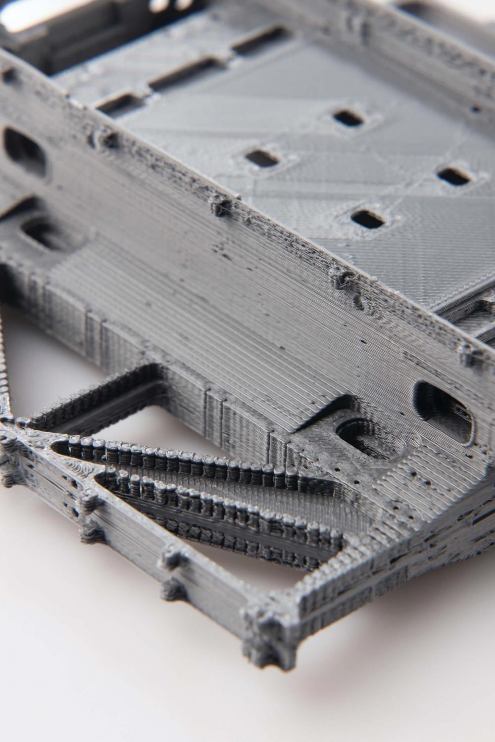
Semi-conductors
Kanigen Group is committed to continuously improving its peripheral processes in meeting the high cleanliness standards required by the semiconductor industry. Today, we have been approved by ASML, Applied Materials, etc.
Our expertise is recognised by equipment manufacturers of semiconductors, 3D printers, scanning microscopes, vacuum applications, as well as by their suppliers.

Protection against corrosion

Anti-static applications

Amorphous

Reduced Friction
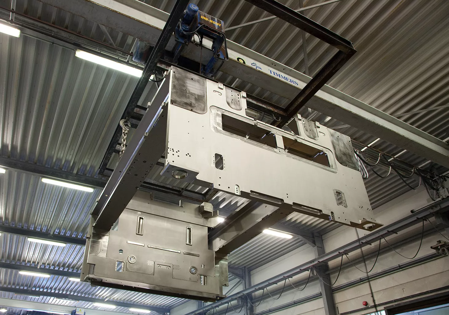
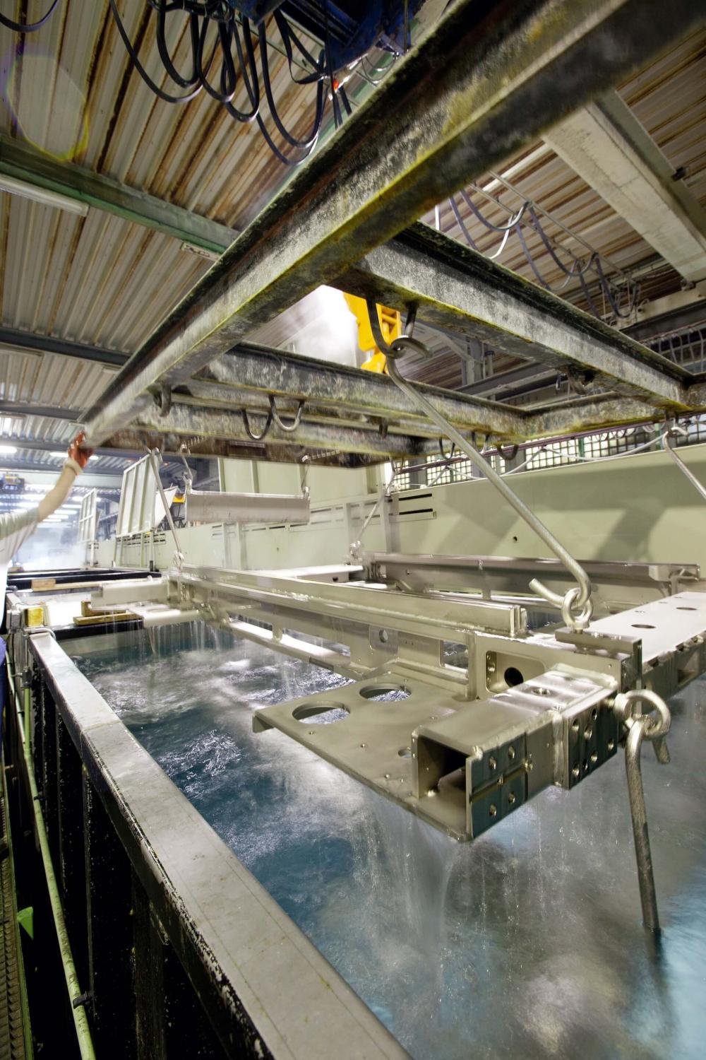
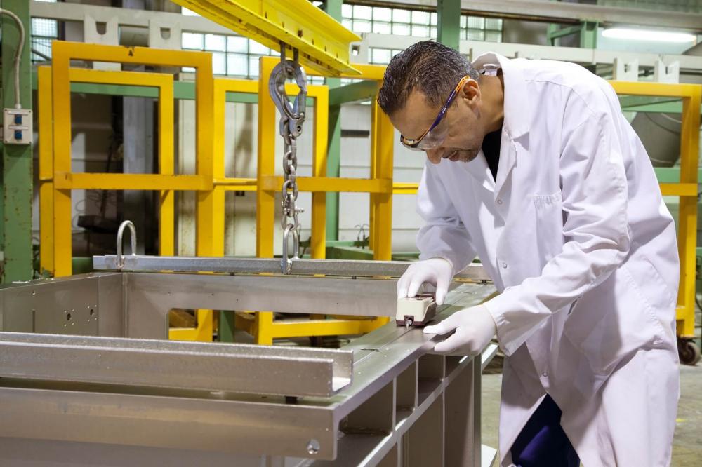
In 2002, Kanigen Group built an electroless nickel line, taking into account the industry's specific cleanliness requirements, to process ASML's steel casings (stepper wafer machines).
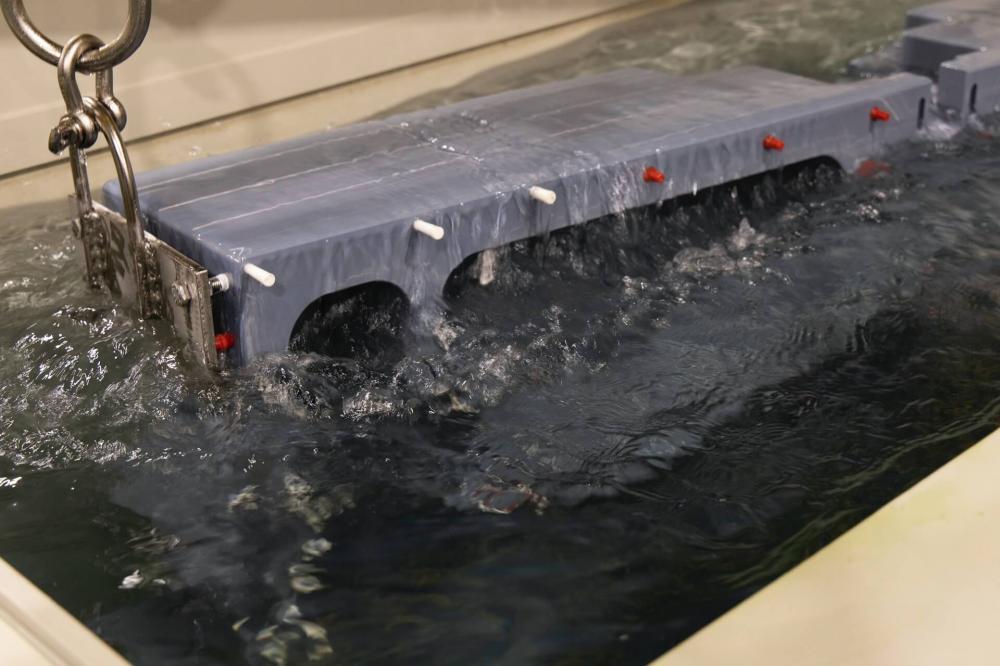
In 2019, this line will be supplemented by an aluminium pre-treatment line, along with a grey room dedicated to the packing of such parts.
Nickel deposition bath dimensions
- Non-alloyed steels: 3,100 x 2,200 x 2,000 mm
- Aluminium: 2,600 x 2,050 x 1,000 mm
- NiPtef and black electroless nickel: 600 x 600 x 1,500 mm
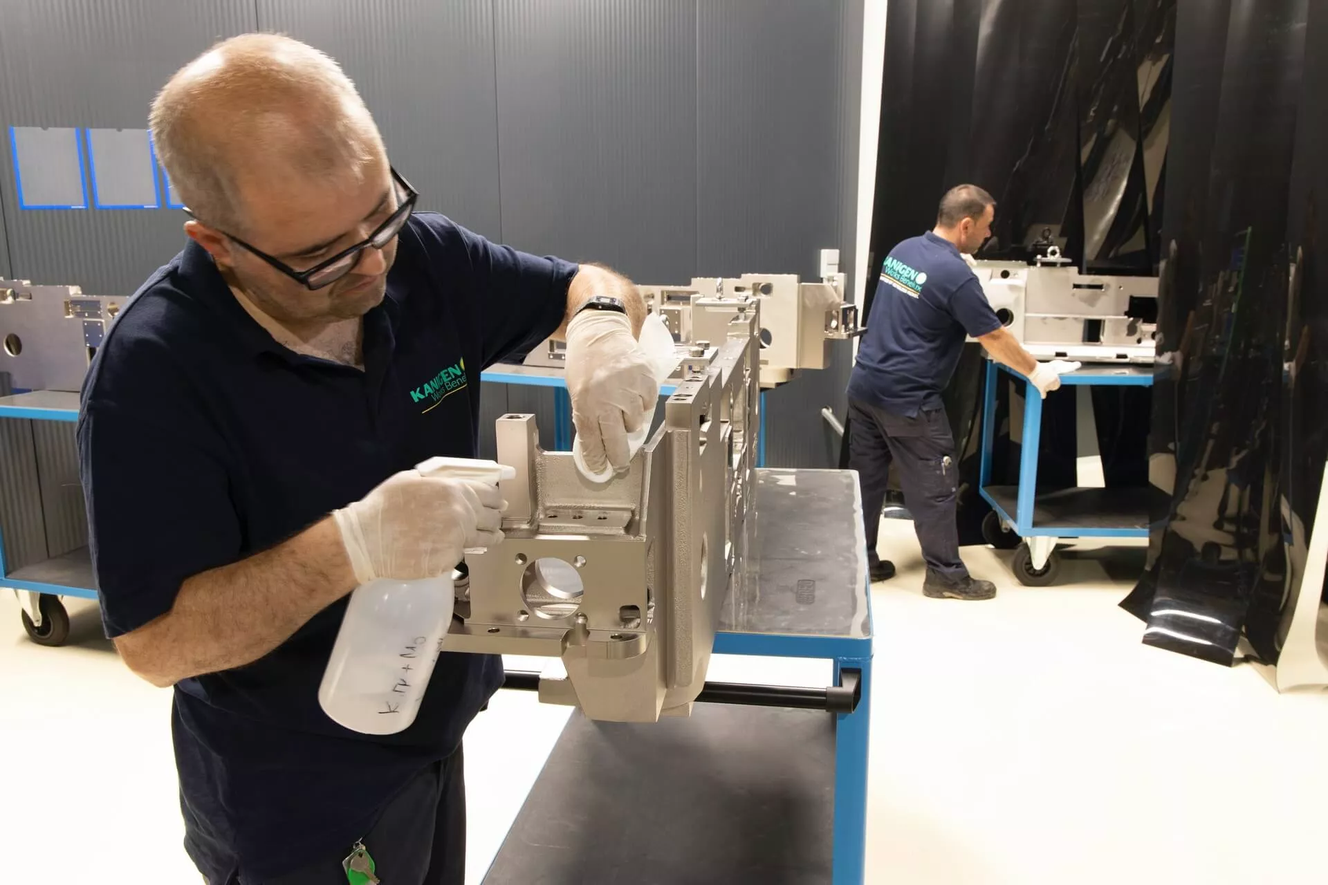
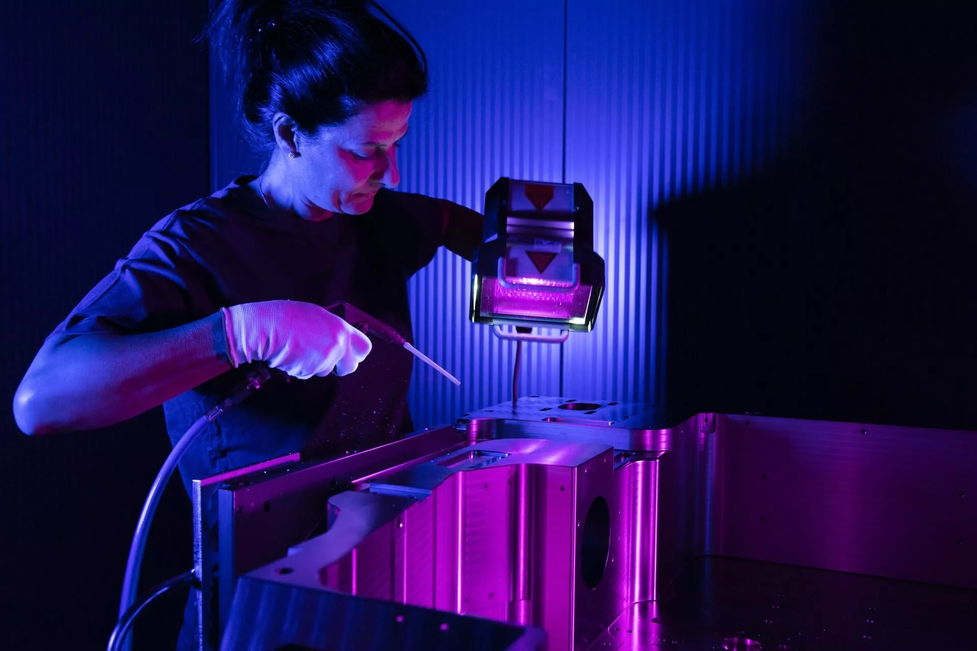
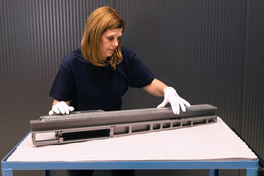
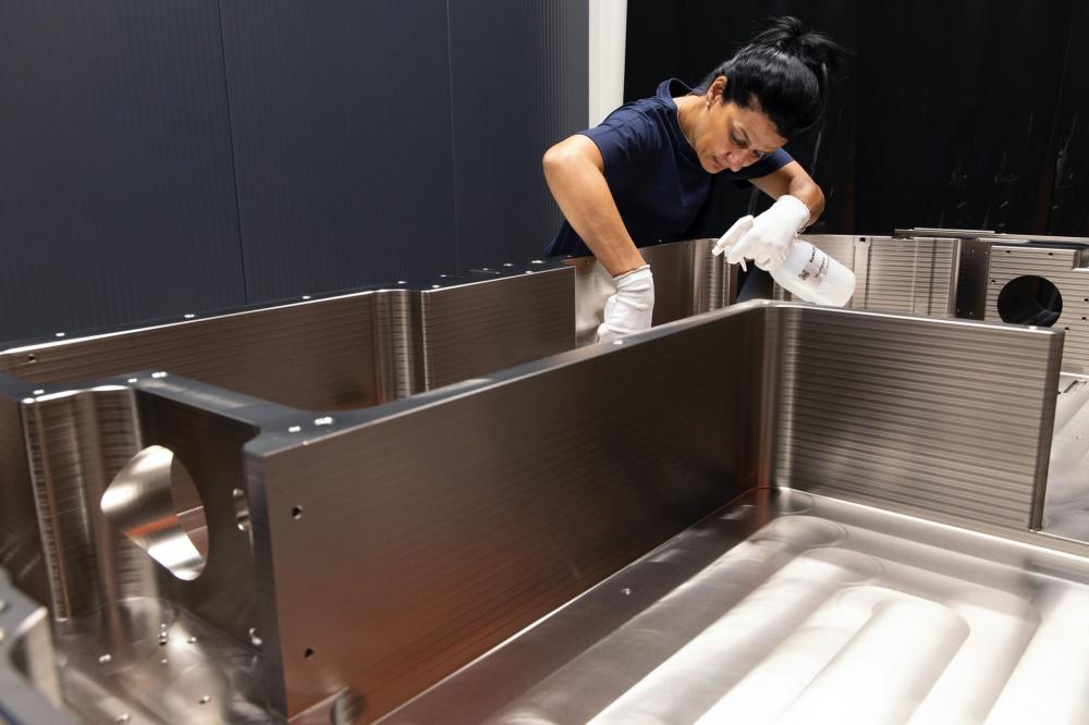
Kanigen Works Benelux is equipped with a grey room, allowing it to handle semiconductor parts that must be packed ‘clean room-compatible’.
It is equipped to meet the ASML standards:
- GSA 07 4320 – Grade 4 – Surface cleanliness
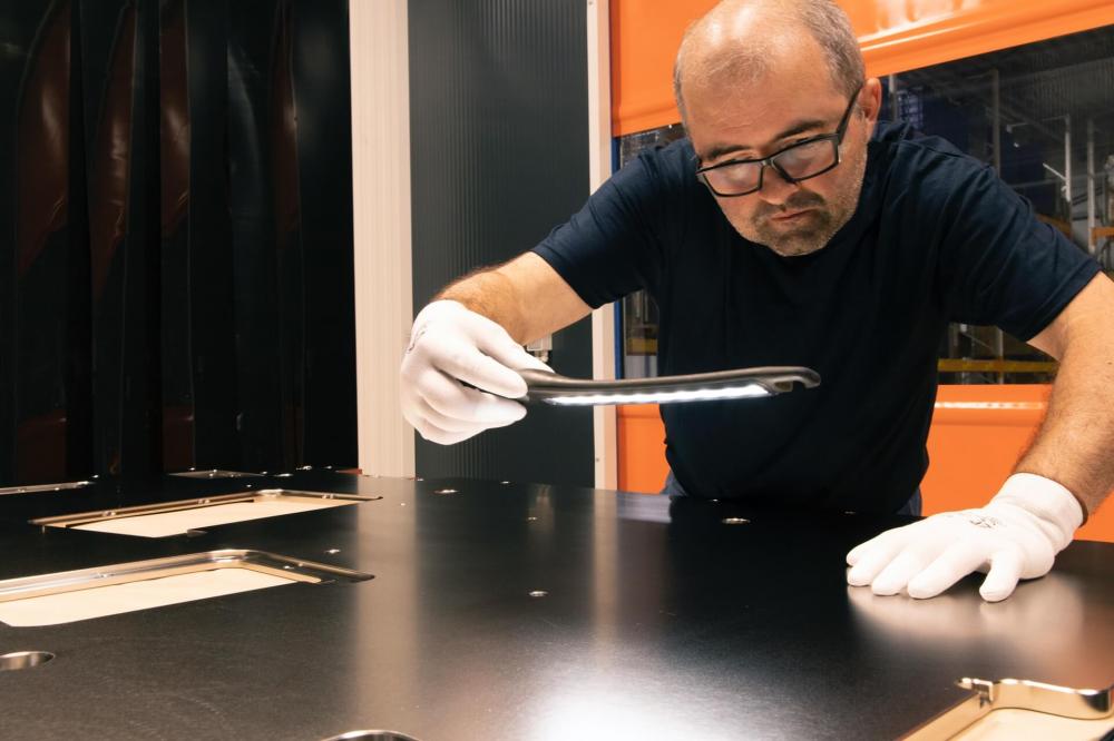
- GSA 07 0011 – Bright light inspection
- GSA 07 0012 – UV-A Blacklight inspection
The nickel plating process as applied at Kanigen Works Benelux is Grade 2 compatible.
Other standards applied: AMAT 0250-07726-027.
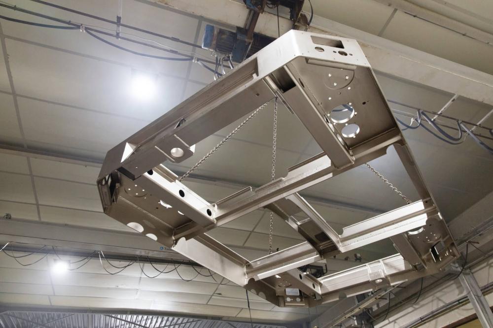
- Machine frames
- Vacuum chambers
- Guidance system parts
- Fastening and mounting systems, etc.
